In today’s technology-driven world, electronic devices are becoming smaller, faster, and more powerful. To meet these demands, Multilayer Printed Circuit Boards (PCBs) have emerged as an essential component in modern electronic design. These complex circuit boards play a vital role in telecommunications, medical devices, automotive, and aerospace industries.
- The global PCB market is projected to exceed $80 billion by 2030.
- 5G deployment is driving demand for high-speed multilayer PCBs.
- The automotive PCB segment is witnessing rapid growth from EV advancements.
Table of Contents
Understanding Multilayer PCBs
What is a Multilayer PCB?
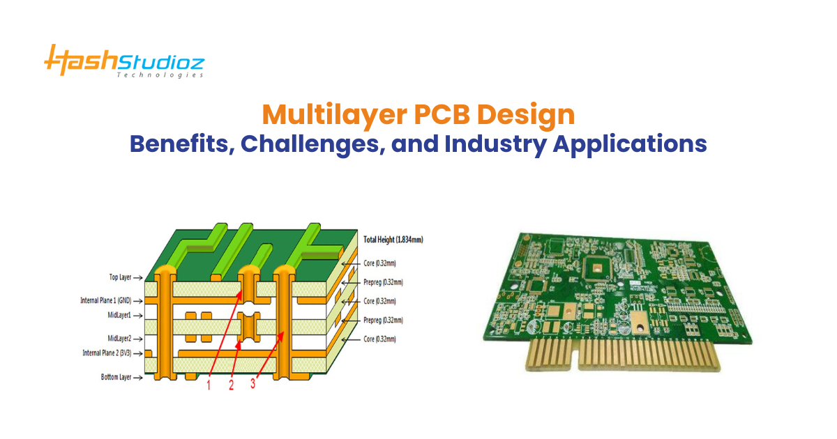
A multilayer PCB (Printed Circuit Board) consists of three or more layers of conductive material, usually copper, separated by insulating layers known as prepreg. Single-layer and double-layer PCBs have one or two copper layers, respectively. Multilayer PCBs incorporate multiple copper layers to support complex circuits and high-speed applications.
These boards are widely used in advanced electronics like medical devices, aerospace systems, telecommunications equipment, and consumer electronics, where compact size, signal integrity, and high performance are essential.
Structure of Multilayer PCBs
Multilayer PCBs are built with multiple layers stacked together in a precise structure. Each layer plays a crucial role in ensuring the board’s electrical and mechanical performance.
Key Components of a Multilayer PCB:
- Core Layers: The central substrate material (often FR4) that provides structural stability.
- Copper Layers: The conductive paths that form electrical circuits and connections.
- Prepreg Layers: Insulating material that separates the copper layers and ensures proper electrical isolation.
- Via Structures: Holes that connect different layers for signal transmission between them.
- Solder Mask: A protective coating applied over the PCB to prevent oxidation and short circuits.
- Silkscreen Layer: Used for component labeling and reference designations.
The stack-up of a multilayer PCB determines its performance, signal integrity, and thermal management.
How Multilayer PCBs are Manufactured
The manufacturing of multilayer PCBs is a complex process requiring precision and advanced technology. Below are the key steps involved:
1. Designing the PCB Layout
- Engineers use specialized PCB design software like Altium Designer, Eagle, or KiCad to create the circuit layout.
- The design includes layer stack-up, component placement, and routing of electrical connections.
- Signal integrity and thermal management considerations are implemented in this phase.
2. Printing Inner Layers
- The circuit pattern for the inner copper layers is printed using a photoresist process.
- Excess copper is etched away, leaving only the desired circuit traces.
3. Layer Lamination Process
- Multiple layers of copper and prepreg are aligned and laminated under heat and pressure.
- This process bonds all layers into a single, solid PCB structure.
4. Drilling and Plating Vias
- Holes are drilled to create vias, which provide electrical connections between layers.
- Common via types include:
- Through-Hole Vias: Extend through the entire board.
- Blind Vias: Connect outer layers to inner layers without passing through the entire PCB.
- Buried Vias: Connect only the inner layers, remaining invisible from the outer layers.
- A copper plating process is used to coat the drilled vias, ensuring proper conductivity.
5. Etching Process
- A chemical etching process removes excess copper from the outer layers, leaving behind the circuit traces.
6. Solder Mask and Surface Finish Application
- The solder mask is applied to protect the copper traces from oxidation and prevent solder bridges.
- A surface finish (such as HASL, ENIG, or OSP) is applied to enhance solderability and corrosion resistance.
7. Quality Inspection and Testing
- Automated Optical Inspection (AOI) checks for defects.
- Electrical Testing (Flying Probe or Bed of Nails) verifies continuity and insulation resistance.
- X-ray Inspection ensures correct via alignment and internal structure.
These steps ensure that the final multilayer PCB meets industry standards for reliability and performance.
Benefits of Multilayer PCBs
Multilayer PCBs offer numerous advantages over single-layer and double-layer PCBs, making them the preferred choice for high-performance and compact electronic applications. Below are the key benefits explained in detail.

1. Compact Size and Space Efficiency
Multilayer PCBs integrate multiple circuit layers within a small and compact footprint, which is crucial for modern electronic devices.
- Unlike traditional single-layer or double-layer PCBs, which require larger board space for routing complex circuits, multilayer PCBs optimize space utilization.
- They enable the development of miniaturized devices such as:
- Smartphones and tablets
- Wearable technology (smartwatches, fitness trackers)
- Medical implants (pacemakers, hearing aids)
- By stacking multiple layers, engineers can incorporate more functionality into a smaller form factor without compromising performance.
2. Enhanced Performance and Signal Integrity
Multilayer PCBs improve signal integrity by reducing electromagnetic interference (EMI) and ensuring stable electrical performance.
- Dedicated power and ground planes help in reducing noise and voltage fluctuations.
- Shorter signal paths minimize resistance and capacitance, improving overall circuit efficiency.
- These characteristics make multilayer PCBs ideal for high-frequency applications, such as:
- Telecommunication systems
- Satellite communication devices
- Radar and defense electronics
3. High-Speed Capabilities
Multilayer PCBs are designed to support high-speed and high-frequency applications by minimizing signal degradation.
- Shorter interconnections reduce transmission delays and signal loss.
- Controlled impedance in the PCB layout ensures stable signal flow.
- Low dielectric constant (Dk) materials further enhance performance in high-speed circuits.
- Industries that benefit from high-speed multilayer PCBs include:
- 5G networks and IoT devices
- Automotive electronics (ADAS, infotainment systems)
- Aerospace and avionics systems
4. Greater Design Flexibility
Multilayer PCBs provide more routing options and design flexibility, enabling engineers to develop complex circuit architectures.
- Unlike single-layer PCBs, where routing space is limited, multilayer PCBs allow for:
- Denser component placement
- Better signal routing using multiple layers
- Reduction of crossover issues
- This flexibility is essential for industries that require customized PCB layouts, such as:
- Medical equipment (MRI, CT scanners)
- AI-driven computing systems
- Industrial automation and robotics
5. Cost-Effectiveness in Large Production Runs
Although multilayer PCBs have a higher initial manufacturing cost, they become cost-effective when produced in bulk due to:
- Reduced component count: More functionalities are integrated into a single PCB, reducing the need for external wiring and components.
- Lower failure rates: Multilayer PCBs offer higher reliability, minimizing the need for replacements and repairs.
- Streamlined assembly process: Advanced manufacturing techniques enable automated assembly, reducing labor costs.
Industries that benefit from bulk production of multilayer PCBs include:
- Consumer electronics (laptops, gaming consoles, smart TVs)
- Medical and healthcare devices
- Automotive and electric vehicle (EV) manufacturers
Choosing the Right PCB Design Software: Altium vs. Eagle vs. KiCAD vs. Orcad
Challenges in Multilayer PCB Design
While multilayer PCBs offer numerous advantages, they also come with significant design and manufacturing challenges. These challenges must be carefully addressed to ensure optimal performance, reliability, and cost-effectiveness. Below are some of the most critical issues faced in multilayer PCB design.
1. Complex Manufacturing Process
The fabrication of multilayer PCBs involves multiple intricate steps, requiring precision, advanced machinery, and strict quality control.
- Multiple layers must be perfectly aligned during the lamination process.
- Via drilling and plating become more complicated, especially for blind and buried vias.
- The increased number of processing steps, including:
- Lamination
- Drilling and plating
- Etching and solder masking
- Testing and quality checks
- Assembly and inspection
- Longer production time compared to single-layer or double-layer PCBs due to additional steps.
Impact: The complexity of manufacturing increases the risk of defects, misalignments, or layer delamination, making quality assurance a crucial part of the production process.
2. Higher Design Costs
Multilayer PCB design is significantly more expensive than simpler PCB configurations due to:
- Specialized design software like Altium Designer, OrCAD, and Cadence Allegro being required.
- Highly skilled engineers needed for designing multilayer stack-ups, routing, and ensuring signal integrity.
- Extensive prototyping and testing required to avoid performance issues before full-scale production.
While the cost of mass production can be justified, small production runs or prototyping remain costly and resource-intensive.
Impact: Businesses with limited budgets may struggle to afford multilayer PCB designs, especially in low-volume production scenarios.
3. Thermal Management Issues
Higher layer density results in greater heat generation, leading to potential overheating issues.
- Multilayer PCBs have more power planes and signal layers, which can trap heat.
- Improper heat dissipation can affect component reliability and lifespan.
- Effective cooling strategies must be integrated, such as:
- Thermal vias for heat dissipation.
- Heat sinks and thermal pads to transfer heat away from critical components.
- Forced air or liquid cooling systems for high-power applications.
Impact: Without proper thermal management, electronic failures and reduced performance become major risks, particularly in industries like automotive, aerospace, and high-performance computing.
4. Signal Interference and Crosstalk
In multilayer PCBs, closely packed conductive layers increase the risk of electromagnetic interference (EMI) and crosstalk.
- High-speed signals can interfere with adjacent traces, affecting signal integrity.
- Power and ground planes must be strategically placed to minimize EMI.
- Controlled impedance and proper trace spacing are required to avoid unwanted electrical noise.
- Shielding techniques such as ground planes, guard traces, and differential pairs must be incorporated.
Impact: If not addressed, signal degradation can cause malfunctions in telecommunication, computing, and RF applications, making precise design essential.
5. Repair and Maintenance Complexity
Due to tightly packed components and multiple layers, diagnosing and repairing faults in multilayer PCBs is significantly more challenging compared to single-layer or double-layer PCBs.
- Traces and vias are embedded within layers, making visual inspection difficult.
- Repairing defective layers often requires complete board replacement, increasing maintenance costs.
- Specialized diagnostic equipment like X-ray inspection is needed to detect internal defects.
Impact: Companies relying on multilayer PCBs must factor in higher maintenance costs and potential downtime for troubleshooting and repairs.
Key Design Considerations for Multilayer PCBs
To ensure optimal performance, reliability, and manufacturability, designers must carefully consider several critical factors when developing multilayer PCBs. These considerations help in reducing signal loss, preventing thermal issues, and enhancing overall circuit integrity.

1. Layer Stack-Up Design
The layer stack-up is the foundation of a multilayer PCB, determining its electrical, thermal, and mechanical properties. A well-structured stack-up improves signal integrity, power distribution, and EMI performance.
Factors to Consider in Stack-Up Design:
- Number of Layers: Deciding between 4-layer, 6-layer, or higher configurations based on circuit complexity.
- Sequence of Layers: Proper arrangement of signal, power, and ground layers to reduce interference.
- Symmetry: Maintaining balanced stack-ups to prevent warping and improve manufacturability.
- Spacing Between Layers: Optimizing the distance between signal layers to control impedance and minimize crosstalk.
Best Practice: Use dedicated power and ground planes between signal layers to enhance signal integrity and reduce electromagnetic interference (EMI).
2. Material Selection
Choosing the right dielectric material is crucial for achieving signal stability, thermal management, and mechanical durability.
Key Material Properties to Consider:
- Dielectric Constant (Dk): Affects signal propagation speed; lower Dk is preferable for high-frequency applications.
- Loss Tangent (Df): Determines signal loss; a lower Df improves performance in RF and high-speed circuits.
- Thermal Conductivity: Ensures efficient heat dissipation in high-power applications.
- Coefficient of Thermal Expansion (CTE): Impacts reliability, especially for temperature-sensitive environments.
Common Materials Used in Multilayer PCBs:
- FR4 (Fiberglass Epoxy): Cost-effective, widely used for standard applications.
- Polyimide: High heat resistance, suitable for aerospace and automotive applications.
- Rogers Material: Preferred for RF, microwave, and high-speed circuits due to lower Dk and Df values.
- Metal-Core PCBs (MCPCBs): Used for LEDs and power electronics for superior heat dissipation.
Best Practice: Choose materials based on the operating frequency, thermal demands, and budget of the PCB application.
3. Via Design and Placement
Vias are essential for connecting different layers in a multilayer PCB. Proper via selection improves electrical performance and manufacturability.
Types of Vias Used in Multilayer PCBs:
- Through-Hole Vias: Extend through the entire PCB; common but may occupy excessive space.
- Blind Vias: Connect outer layers to inner layers without passing through the entire board; saves space.
- Buried Vias: Connect only inner layers, improving routing efficiency for complex designs.
- Microvias: Laser-drilled vias used in HDI (High-Density Interconnect) PCBs for fine-pitch designs.
Factors to Consider in Via Placement:
- Minimizing Via Inductance: Shorter vias reduce signal degradation in high-speed circuits.
- Via-in-Pad Design: Helps in saving space and improving signal integrity but requires specialized fabrication.
- Thermal Vias: Placed near heat-generating components to aid in heat dissipation.
Best Practice: Use blind and buried vias for high-density PCBs, and optimize via placement to maintain mechanical strength and electrical performance.
4. Power Distribution and Ground Planes
Proper power distribution and grounding are crucial for ensuring stable voltage delivery and minimizing electrical noise.
Key Considerations for Power and Ground Design:
- Dedicated Power and Ground Planes: Reduce voltage fluctuations and improve power integrity.
- Minimizing Return Paths: Ensure short and direct return paths to prevent noise and interference.
- Use of Decoupling Capacitors: Placed near ICs to stabilize power supply and filter noise.
- Avoiding Split Planes: Sudden changes in power/ground plane continuity can cause signal integrity issues.
Best Practice: Design continuous, low-impedance power and ground planes for better EMI/EMC performance and noise reduction.
5. EMI/EMC Considerations
Multilayer PCBs must be designed to minimize electromagnetic interference (EMI) and ensure electromagnetic compatibility (EMC) for regulatory compliance.
Techniques to Reduce EMI and Enhance EMC:
- Ground and Power Layer Shielding: Placing signal layers between power/ground planes helps contain EMI.
- Controlled Impedance Routing: Ensures consistent signal transmission in high-speed designs.
- Use of Guard Traces and Faraday Shielding: Reduces noise in sensitive circuits.
- Proper Trace Spacing: Maintains adequate distance between high-speed traces to reduce crosstalk.
- Differential Pair Routing: Used in USB, HDMI, and RF circuits to improve noise immunity.
Best Practice: Simulate EMI performance using PCB design software before manufacturing to ensure compliance with FCC, CE, and industry standards.
Designing PCBs for IoT Devices: Low-Power, High-Density Layout Strategies
Industry Applications of Multilayer PCBs
Multilayer PCBs are widely used across industries for their compact size, high performance, and ability to support complex circuitry. Their reliability and efficiency make them essential for applications requiring high-speed processing, signal integrity, and durability. Below are the key industries that rely on multilayer PCB technology.
1. Consumer Electronics
Consumer electronics require compact, high-performance, durable PCB designs to accommodate advanced functionalities and maintain sleek, portable designs.
Common Consumer Electronics Using Multilayer PCBs:
- Smartphones and Tablets:
- Multilayer PCBs enable thin, lightweight, and energy-efficient designs.
- Support for high-speed data transfer and wireless connectivity (Wi-Fi, Bluetooth, 5G).
- Laptops and Computers:
- Used in motherboards, graphic cards, and processors for high-speed computing.
- Gaming Consoles and VR Devices:
- Multilayer PCBs support complex graphics processing and high-speed gaming performance.
- Smart Home Devices:
- Found in smart TVs, home automation systems, and IoT-based devices.
Why Multilayer PCBs?
- Compact form factor
- High-speed data transmission
- Better heat dissipation for prolonged use
2. Telecommunications
Telecommunication systems rely on multilayer PCBs to maintain signal integrity, high-frequency operations, and uninterrupted data transmission.
Key Applications in Telecommunications:
- 5G Infrastructure & Base Stations:
- Multilayer PCBs help handle high-frequency, low-latency, and high-speed data transmission.
- Networking Equipment (Routers, Switches, Servers):
- Require stable power distribution, noise reduction, and signal integrity.
- Satellite Communication Systems:
- High-reliability PCBs are needed for long-distance signal transmission.
Why Multilayer PCBs?
- Support for high-speed, high-frequency signals
- Reduced electromagnetic interference (EMI)
- Long-term reliability in harsh environments
3. Aerospace and Defense
Multilayer PCBs are essential for high-reliability applications in aerospace and defense, where precision, durability, and safety are critical.
Common Aerospace and Defense Applications:
- Avionics Systems:
- Used in flight control systems, navigation, and communication equipment.
- Radar and Sonar Systems:
- Multilayer PCBs help process high-speed signals with minimal interference.
- Satellite Systems and Space Exploration:
- Require radiation-resistant, thermally stable, and lightweight PCBs.
- Military Equipment (Missile Guidance, Surveillance Systems):
- Need highly durable and failure-resistant PCB solutions.
Why Multilayer PCBs?
- Extreme reliability in high-altitude and space conditions
- High resistance to thermal expansion and environmental stress
- Strong signal integrity for mission-critical applications
4. Automotive Industry
Modern automobiles depend on multilayer PCBs for advanced electronic systems that enhance safety, efficiency, and user experience.
Key Automotive Applications:
- Advanced Driver Assistance Systems (ADAS):
- Enables collision avoidance, adaptive cruise control, and lane departure warning.
- Infotainment & Navigation Systems:
- High-speed PCBs support GPS, touchscreens, and multimedia systems.
- Electric Vehicles (EVs) & Battery Management Systems:
- Multilayer PCBs manage power distribution, energy storage, and motor control.
Why Multilayer PCBs?
- Withstand vibrations, temperature variations, and high-power demands
- Enable compact, lightweight designs
- Improve energy efficiency and vehicle automation
5. Medical Devices
Multilayer PCBs are critical in medical technology, where precision, reliability, and miniaturization are required for patient safety and effective diagnostics.
Common Medical Applications:
- Medical Imaging Equipment (MRI, CT, X-Ray):
- High-performance PCBs ensure accurate imaging and signal processing.
- Wearable Health Monitors (Smartwatches, Fitness Trackers):
- Compact multilayer PCBs enable continuous heart rate and ECG monitoring.
- Implantable Medical Devices (Pacemakers, Hearing Aids):
- Require biocompatible, power-efficient, and highly durable PCBs.
- Surgical Equipment & Robotic-Assisted Surgery:
- High-reliability PCBs are used in robotic surgical instruments.
Why Multilayer PCBs?
- Support for miniaturized, lightweight medical devices
- High durability in critical healthcare environments
- Superior signal processing for accurate diagnostics
6. Industrial Equipment
Industrial automation and power electronics require multilayer PCBs for high-performance, durable, and efficient operation in harsh environments.
Key Industrial Applications:
- Factory Automation & Robotics:
- Used in AI-powered robots, PLCs (Programmable Logic Controllers), and motor controls.
- Power Electronics & Renewable Energy:
- Multilayer PCBs support solar inverters, wind turbines, and battery management systems.
- Heavy Machinery & Sensors:
- Rugged PCBs power sensors, actuators, and industrial-grade electronics.
Why Multilayer PCBs?
- Enhanced durability against high temperatures, moisture, and vibrations
- High reliability for continuous operation in industrial environments
- Support for power-intensive applications
PCB Design for Medical Devices: Compliance with FDA and IEC 60601 Standards
PCB Design Services: Why They Matter
Professional PCB Design Services play a vital role in helping businesses develop high-quality, error-free, and efficient PCB designs that meet industry standards. These services bridge the gap between concept and production, ensuring that the final product is optimized for functionality, cost-effectiveness, and scalability.
1. Optimized Design for Performance & Reliability
- Precision Engineering: Professional designers ensure optimized component placement, trace routing, and power distribution to enhance performance.
- Signal Integrity: Expert PCB layout techniques reduce signal interference, crosstalk, and electromagnetic interference (EMI).
- Thermal Management: Advanced design services incorporate effective heat dissipation solutions, preventing overheating and component failure.
2. Reduced Design Errors & Faster Time to Market
- Design Rule Checks (DRC): Automated checks identify potential errors early, preventing costly revisions.
- Prototyping & Simulation: Virtual testing ensures the design is functionally sound prior to manufacturing.
- Iterative Improvements: PCB design experts refine the design based on real-world testing and industry best practices.
3. Cost-Effective Manufacturing
- Material & Component Optimization: Expert PCB designers choose cost-effective materials and components without compromising quality.
- Manufacturing Feasibility: Designs are tailored to streamline production, reducing fabrication complexity and costs.
- Minimized Waste: Efficient layout techniques ensure optimal use of PCB real estate, reducing material waste.
4. Scalability & Customization for Various Applications
- Custom PCB Design: Tailored solutions for high-frequency, high-power, or miniaturized electronics.
- Scalability for Mass Production: Ensures that the design is ready for high-volume manufacturing with consistent quality.
- Multi-Industry Support: PCB design services cater to industries ranging from IoT and AI to medical and automotive electronics.
Choosing the Right Multilayer PCB Design Partner
Selecting the right Multilayer PCB design service provider is crucial for ensuring the success of your project. Here are the key factors to consider:
1. Experience & Expertise
- Look for proven experience in designing multilayer, high-speed, and custom PCBs.
- Evaluate expertise in advanced design software like Altium Designer, KiCad, and OrCAD.
- Consider industry-specific experience in automotive, aerospace, or medical PCB design.
2. Technological Capabilities
- Ensure the provider offers state-of-the-art simulation, prototyping, and testing tools.
- Check for experience with High-Density Interconnect (HDI) PCBs, flexible PCBs, and RF PCB designs.
- Look for expertise in designing for manufacturability (DFM) and assembly (DFA).
3. Quality Assurance & Compliance
- Confirm the provider follows industry standards like IPC, ISO, and UL certifications.
- Ensure rigorous testing protocols: signal integrity analysis, thermal testing, and EMI/EMC testing.
- Ask about reliability validation for harsh environments such as temperature, humidity, and vibration resistance.
4. Scalability & Production Support
- The right partner should support small-scale prototyping and large-scale production.
- Check if they provide turnkey PCB solutions, including design, fabrication, and assembly.
- Look for a provider with a global supply chain to ensure component availability and cost efficiency.

Conclusion
Multilayer PCB design is a cornerstone of modern electronics, offering space efficiency, performance enhancement, and design flexibility. While challenges exist, proper design strategies and PCB Design Services help in overcoming them. As industries continue to evolve, multilayer PCBs will play a crucial role in advancing technology.
FAQs
What are the advantages of multilayer PCBs over single-layer PCBs?
Multilayer PCB design offers superior performance, better signal integrity, and higher space efficiency compared to single-layer PCBs. The stacked layers in multilayer PCB design reduce electromagnetic interference (EMI) and enhance electrical properties, making them ideal for high-speed circuits.
What industries benefit the most from multilayer PCBs?
Industries such as consumer electronics, telecommunications, automotive, aerospace, and medical heavily depend on multilayer PCB design for compact, high-density circuits. Multilayer PCB design is crucial for applications requiring miniaturization, high-frequency performance, and enhanced durability.
How do PCB Design Services enhance multilayer PCB development?
Professional multilayer PCB design services optimize layout, ensure manufacturability, and improve thermal management. These services also assist in prototyping, fabrication, and quality assurance, leading to more reliable and efficient multilayer PCB design solutions.